Power Semiconductors Weekly Vol. 36
Hitachi Develops Highly Flexible Design Technology Based on Physical Model of TED-MOS SiC Power Device
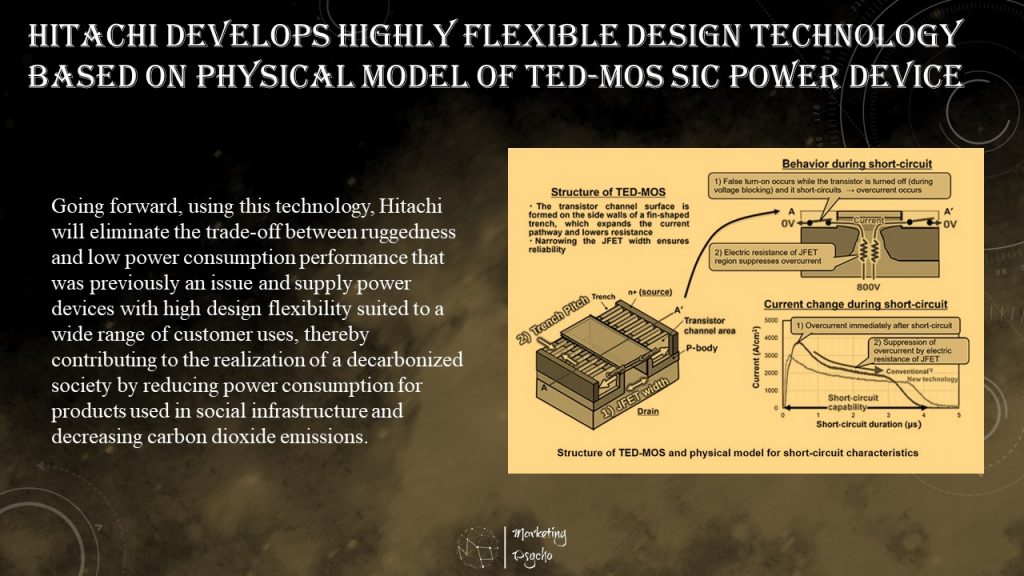
With the aim of helping achieve a decarbonized society, Hitachi previously developed TED-MOS, a power device with an innovative structure that uses the next-generation material silicon carbide (SiC) and delivers improved ruggedness and low power consumption characteristics. It has now established a physical model relating to the suppression mechanism for overcurrent, which causes breakdowns when a device short-circuits. Furthermore, based on this physical model, it has developed highly flexible device design technology that leverages the structural advantages of TED-MOS.
This has made it possible to eliminate the trade-off between ruggedness and low power consumption characteristics that is an issue with conventional power devices that incorporate silicon-based materials, thereby supporting increased energy-efficiency and energy-saving performance for power electric devices used for a wide range of purposes by customers. Going forward, Hitachi aims to further improve the performance of TED-MOS and develop a wide range of applications for the product, such as energy systems, electrical vehicles, and data centers.
Because SiC power devices have higher dielectric breakdown electric field strength compared with conventional devices that use silicon (Si), it is possible to reduce the thickness of the devices, making them suitable for low-resistance, high-frequency switching. However, the following is an issue: because the dielectric breakdown electric field strength is high when the device is turned off, it is difficult to ensure the product’s lifetime if a short-circuit occurs due to a malfunction.

In order to resolve this issue, Hitachi has established a physical model for suppressing overcurrent by focusing on the behavior of the current during a short-circuit, especially the phenomenon of overcurrent due to the short-circuit attenuating after it peaks. Here, the length of time after overcurrent occurs during which the device is able to withstand it without a breakdown is defined as the “short-circuit capability,” which is used as an indicator representing ruggedness. The process via which a device short-circuits may be viewed as follows: 1) overcurrent flows due to the transistor status falsely becoming on while the device is turned off (while the voltage is being blocked); 2) the current density of the JFET in the device’s center increases and the temperature rises locally; and 3) the JFET resistance grows due to the rise in temperature and the overcurrent attenuates. To improve the short-circuit capability, it is necessary to suppress overcurrent, which causes device breakdown.
Typically, the greater the electrical resistance of the transistor region, the lower the overcurrent will be during a short-circuit, so the electrical resistance of the transistor region and short-circuit capability may be considered to have a trade-off relationship. However, if, based on the physical model of item 3 above which is the focus here, it was possible to develop a structure with which there was a significant increase in resistance due to JFET heat generation when a device short-circuits, it would be possible to reduce overcurrent during the short-circuit and there would be no growth in the electrical resistance of the transistor region, enabling improvement of the short-circuit capability.
Going forward, using this technology, Hitachi will eliminate the trade-off between ruggedness and low power consumption performance that was previously an issue and supply power devices with high design flexibility suited to a wide range of customer uses, thereby contributing to the realization of a decarbonized society by reducing power consumption for products used in social infrastructure and decreasing carbon dioxide emissions.
Tandem Diodes for Faster Switching
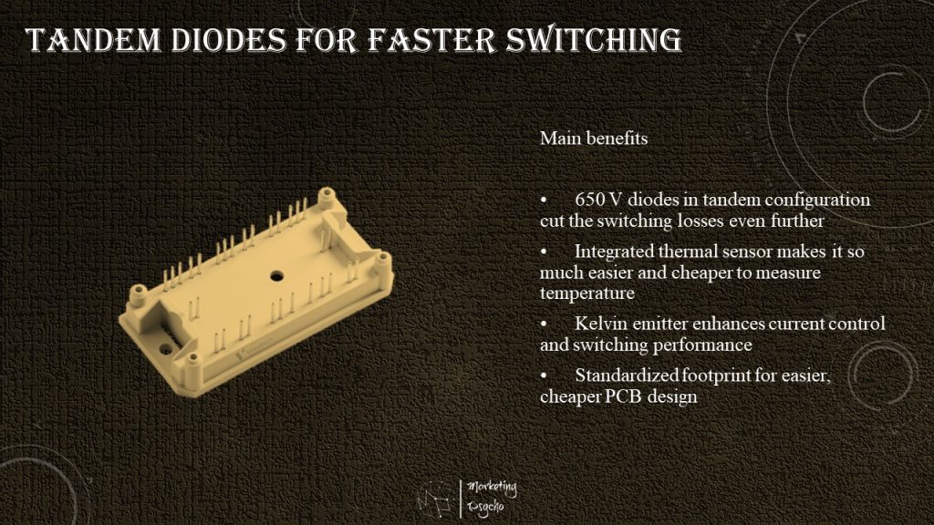
Tandem diodes for power modules equal performance, robustness and cost-effective solutions. For Motion Control market, Vincotech offers Tandem diodes in SixPack, Twin SixPacks and PIM topologies using several housing options. Tandem diode solution reduces further the power losses and assure a long-life cycle of the products.
Main benefits
- 650 V diodes in tandem configuration cut the switching losses even further
- Integrated thermal sensor makes it so much easier and cheaper to measure temperature
- Kelvin emitter enhances current control and switching performance
- Standardized footprint for easier, cheaper PCB design

Applications
- Industrial
- Embedded
Showa Denko Concludes Long-Term Contract to Supply SiC Epitaxial Wafers for ROHM
Showa Denko K.K. (SDK) has concluded a long-term supply contract with ROHM, a Japanese semiconductor manufacturer providing highly efficient SiC power semiconductors for the global market, to supply SiC epitaxial wafers for power semiconductors (SiC epi-wafers) for plural years.
ROHM decided to conclude this long-term contract because the company appreciated high-quality and stable supply system of SDK’s SiC epi-wafers. ROHM continues developing state-of-the-art semiconductors, and therefore, this long-term contract will further strengthen technical cooperation between SDK and ROHM on improvement in qualities of SiC epi-wafers including homogeneity in properties and low density of surface defects.
SDK’s SiC epi-wafers, which were launched into the market in 2009, have been adopted by electronic device manufacturers as parts of various devices including power supply for servers of cloud computing systems, inverters for railcars and solar power generation systems, and converters installed in quick charging stands for EVs. SDK expects that its SiC epi-wafer business will grow further in the market for SiC power devices which is expected to grow very much.
As the largest independent manufacturer of SiC epi-wafers (estimated by SDK), and under a motto of “Best in Class,” the Showa Denko Group will continue coping with rapid expansion of the market for SiC epi-wafers and providing the market with high-performance and highly-reliable products, thereby contributing to the propagation of SiC power semiconductors which save energy with small power loss and less heat generation.
Global Fab Equipment Spending Forecast to Reach $100B in 2022
Powered by digital transformation and other secular technology trends, global semiconductor equipment investments for front end fabs in 2022 are expected to reach nearly $100 billion to meet soaring demand for electronics after topping a projected $90 billion this year, both new records, SEMI highlighted in its World Fab Forecast report.
The new fab equipment spending records will mark a rare three consecutive years of growth that began in 2020, bucking the historical cyclical trend of a one- or two-year expansion followed by a year or two of tepid growth or declines. The semiconductor industry last saw more than two consecutive years of growth in the mid-1990s.
The foundry sector will account for the bulk of fab equipment investments in 2022, with more than $44 billion in spending, followed by the memory sector at over $38 billion. Both DRAM and NAND also show large increases in 2022 with jumps in spending to $17 billion and $21 billion, respectively. Micro/MPU investments will reach approximately $9 billion, discrete/power $3 billion, analog $2 billion, and other devices about $2 billion next year.
Regionally in 2022, Korea will lead in fab equipment spending at $30 billion, followed by Taiwan at $26 billion, and China at nearly $17 billion. Japan will take the fourth spot with almost $9 billion in fab equipment spending. While Europe/Mideast will be in fifth place at US$8 billion, the region is expected to post standout year-over-year percentage growth of 74% in 2022. In the Americas and Southeast Asia, spending is projected to reach more than $6 billion and $2 billion.
Hangzhou Semiconductor Wafer Has Successfully Completed Financing
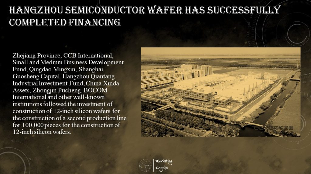
Hangzhou Semiconductor Wafer Co., Ltd has successfully completed financing with a funding volume of 3.3 billion CNY. Zhejiang Province, CCB International, Small and Medium Business Development Fund, Qingdao Mingxin, Shanghai Guosheng Capital, Hangzhou Qiantang Industrial Investment Fund, China Xinda Assets, Zhongjin Pucheng, BOCOM International and other well-known institutions followed the investment of construction of 12-inch silicon wafers second production line for 100,000 pieces. By the end of 2022, 12-inch silicon wafers production will achieve capacity of 200,000 pieces per month.

Vincotech Webinar: Design Challenges and Solutions for 1,500 V PV Inverter Systems
Renewable energy is the gateway to a cleaner future, and solar power is leading the charge. Engineers who design solar inverters face the multidimensional challenge of making sure solar power will continue to meet growing demand for clean energy. This Vincotech webinar explores many facets of this challenge by comparing the latest solutions’ efficiency, weight, and cost, and demonstrating how flying capacitor topologies present unique opportunities for optimizing systems.
Vincotech’s latest generation of power modules for the solar market is underpinned by new design concepts tailored to meet the key requirements of high efficiency, maximum power density, low weight, and great reliability. The company’s engineers chose the innovative topologies and latest semiconductors best suited to benefit the overall system. This webinar dives deep to analyze the power conversion steps in an inverter, and show where and how Vincotech’s latest modules address these design requirements.
Performance and cost comparisons underscore that flying capacitor topologies in the booster and inverter greatly improve efficiency, cut module and system costs, and reduce weight in the inductor and heat sink. With these new topologies, designers of next-generation PV inverter systems are able to meet the four critical design requirements of high efficiency, maximum power density, low weight, and great reliability.
Key Takeaways
- Explore the latest developments in 1,500 V PV inverter topology
- Get to know Vincotech’s latest baseplate-less housing tailored for solar applications
- Discover an end-to-end system solution for the booster and inverter stage
- Learn how flying capacitor topologies can help reduce inductor size and cost
- Date: September 22, 2021
- Time: 8 AM EDT (5 AM PDT / 2:00 PM CEST)
- Duration: 1 hour
Infineon Webinar: Power Semiconductor Solutions for Propulsion and Auxiliaries in Trucks, Delivery Vehicles and Buses
Targets set in emissions standards in many parts of the world to reduce greenhouse gas and pollutant emissions from transport have brought electric propulsion to the fore in recent years and is revolutionizing transport. In addition to passenger cars, more and more commercial vehicles such as trucks, buses and vans, as well as agricultural and construction vehicles, are being powered electrically. This makes them more environmentally friendly, quieter and more efficient than their predecessors with combustion engines.

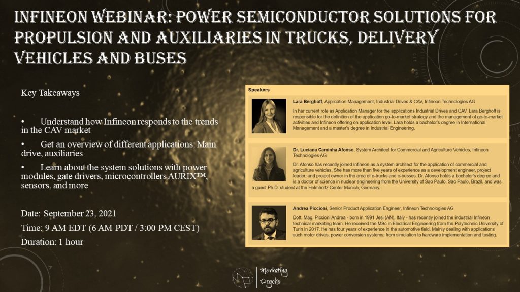
Infineon covers the entire spectrum of heavy-duty vehicle electrification. With proven expertise and a comprehensive portfolio of robust, high-quality control and power semiconductor solutions, Infineon supports developing successful and reliable designs for commercial, construction and agricultural vehicles. In this Infineon webinar, you will learn more about Infineon’s solutions consisting of Si IGBT and CoolSiC™ MOSFETs, discretes and power modules as well as complementary gate drivers, microcontrollers and current sensors.
Key Takeaways
- Understand how Infineon responds to the trends in the CAV market
- Get an overview of different applications: Main drive, auxiliaries
- Learn about the system solutions with power modules, gate drivers, microcontrollers AURIX™, sensors, and more
- Date: September 23, 2021
- Time: 9 AM EDT (6 AM PDT / 3:00 PM CEST)
- Duration: 1 hour
Subscribe to Power Semiconductors Weekly and watch it on YouTube every Tuesday.
If you prefer a monthly update about the world of power semiconductors delivered to your e-mail address, please, subscribe to Marketing Psycho Power Semiconductors newsletter.
